 | –≠–ª–µ–∫—Ç—Ä–æ–Ω–Ω—ã–π –∫–æ–º–ø–æ–Ω–µ–Ω—Ç: SP526CF | –°–∫–∞—á–∞—Ç—å:  PDF PDF  ZIP ZIP |

1
Rev: B Date:7/7/04
SP526 Multi≠Mode Serial Transceiver
© Copyright 2004 Sipex Corporation
SP526
WAN Multi-Mode Serial Transceiver
DESCRIPTION
The SP526 is a monolithic device that sup-
ports three (3) physical layer serial interface
standards. The SP526 is fabricated using a
low power BiCMOS process technology, and
incorporates four (4) drivers and four (4)
receivers can be configured via software for
the selected interface modes at any time.
The SP526 includes tri-state ability for the
driver and receiver outputs through separate
enable lines. A shutdown mode is also
included through the mode select pins for
power savings. When mated with the SP322
V.11/V.35 Programmable Transceiver, the
SP526 provides the four (4) channels needed
for handshaking/control lines such as CTS,
RTS, etc. The two transceiver ICs are an
ideal solution for WAN serial ports in
networking equipment such as routers,
DSU/CSU's, and other access devices.
Low-Cost Programmable Serial Transceiver
Four (4) Drivers and Four (4)) Receivers
Driver and Receiver Tri-state Control
Software Selectable Protocol Selection
Interface Modes:
RS-232
(V.28)
RS-422
(V.11, X.21)
EIA-530 or RS-449
(V.10, V.11)
Designed to Meet All NET1/2 Compliancy
Requirements
High ESD Tolerance
±
15kV per Human Body Model
±
15kV per IEC1000-4-2 Air Discharge
±
8kV per IEC1000-4-2 Contact Discharge
T1
T2
T3
R1
R2
R3
T4
R4
SP526
1.0
µ
F
1.0
µ
F
1.0
µ
F
1.0
µ
F
C2≠
1.0
µ
F
C1+
C1≠
C2+
T1IN
8
ENT1
12
T1OUTA
T1OUTB
T2OUTA
T2OUTB
T2IN
ENT2
ENT3
ENT4
T3IN
T3OUTB
T3OUTA
T4OUT
R1OUT
R2OUT
R3OUT
R4OUT
ENR4
ENR3
ENR1
ENR2
R1INA
R2INA
R3INA
R4INA
R3INB
R4INB
R2INB
R1INB
D0
D1
21
17
19
16
7
11
6
10
5
9
35
4
34
3
33
2
32
1
18
14
13
20
15
22
25
24
27
26
29
28
30
43
42
41
40
39
38
37
36
23
44
31
V
DD
V
CC
V
CC
+5V
V
SS
GND
GND
GND
T4IN
Æ
SP526
33
32
31
30
29
28
27
26
25
24
23
1
2
3
4
5
6
7
8
9
10
11
12
13
14
15
16
17
18
19
20
21
22
44
43
42
41
40
39
38
37
36
35
34
ENR4
ENR3
ENR2
ENR1
T4IN
T3IN
T2IN
T1IN
ENT4
ENT3
ENT2
ENT1
D1
D0
V
SS
C2-
C1-
GND
C2+
V
DD
C1+
V
CC
R3OUT
R4OUT
V
CC
T4OUT
T3OUTA
T3OUTB
T2OUTA
T2OUTB
T1OUTA
T1OUTB
GND
GND
R1INA
R1INB
R2INA
R2INB
R3INA
R3INB
R4INA
R4INB
R1OUT
R2OUT
Now Available in Lead Free Packaging

2
Rev: B Date:7/7/04
SP526 Multi≠Mode Serial Transceiver
© Copyright 2004 Sipex Corporation
-
T
A
= +25
∞
C and V
CC
= +4.75V to +5.25V unless otherwise noted.
PARAMETER
MIN.
TYP.
MAX.
UNITS
CONDITIONS
LOGIC INPUTS
V
IL
0.8
Volts
V
IH
2.0
Volts
LOGIC OUTPUTS
V
OL
0.4
Volts
I
OUT
= ≠ 3.2mA
V
OH
2.4
Volts
I
OUT
= 1.0mA
V.28 DRIVER
DC Parameters
Outputs
Open Circuit Voltage
±
15
Volts
per Figure 1
Loaded Voltage
±
5.0
±
15
Volts
per Figure 2
Short-Circuit Current
±
100
mA
per Figure 4
Power-Off Impedance
300
per Figure 5
AC Parameters
V
CC
= +5V for AC parameters
Outputs
Transition Time
1.5
µ
s
per Figure 6; +3V to -3V
Instantaneous Slew Rate
30
V/
µ
s
per Figure 3
Propagation Delay
t
PHL
0.5
1
5
µ
s
t
PLH
0.5
1
5
µ
s
Max.Transmission Rate
120
230
kbps
V.28 RECEIVER
DC Parameters
Inputs
Input Impedance
3
7
k
per Figure 7
Open-Circuit Bias
+2.0
Volts
per Figure 8
HIGH Threshold
1.7
3.0
Volts
LOW Threshold
0.8
1.2
Volts
AC Parameters
V
CC
= +5V for AC parameters
Propagation Delay
t
PHL
50
100
500
ns
t
PLH
50
100
500
ns
ABSOLUTE MAXIMUM RATINGS
These are stress ratings only and functional operation
of the device at these ratings or any other above those
indicated in the operation sections of the specifications
below is not implied. Exposure to absolute maximum
rating conditions for extended periods of time may
affect reliability.
V
CC
............................................................................+7V
Input Voltages:
Logic...............................-0.3V to (V
CC
+0.5V)
Drivers............................-0.3V to (V
CC
+0.5V)
Receivers........................................
±
15.5V
Output Voltages:
Logic................................-0.3V to (V
CC
+0.5V)
Drivers................................................
±
15V
Receivers........................-0.3V to (V
CC
+0.5V)
Storage Temperature..........................-65∞C to +150∞C
Power Dissipation
(derate 14.3mW/∞C above 70∞C)................1144mW
STORAGE CONSIDERATIONS
Due to the relatively large package size of the 44-pin
quad flat-pack, storage in a low humidity environment
is preferred. Large high density plastic packages are
moisture sensitive and should be stored in Dry Vapor
Barrier Bags. Prior to usage, the parts should remain
bagged and stored below 40
∞
C and 60%RH. If the
parts are removed from the bag, they should be used
within 48 hours or stored in an environment at or below
20%RH. If the above conditions cannot be followed,
the parts should be baked for four hours at 125
∞
C
in order remove moisture prior to soldering. Sipex ships
the 44-pin QFP in Dry Vapor Barrier Bags with
a humidity indicator card and desiccant pack. The
humidity indicator should be below 30%RH.
ELECTRICAL CHARACTERISTICS

3
Rev: B Date:7/7/04
SP526 Multi≠Mode Serial Transceiver
© Copyright 2004 Sipex Corporation
T
A
= +25
∞
C and V
CC
= +4.75V to +5.25V unless otherwise noted.
PARAMETER
MIN.
TYP.
MAX.
UNITS
CONDITIONS
V.28 RECEIVER (continued)
AC Parameters (cont.)
Max.Transmission Rate
120
230
kbps
V.10 DRIVER
DC Parameters
Outputs
Open Circuit Voltage
±
4.0
±
6.0
Volts
per Figure 9
Test-Terminated Voltage
0.9V
OC
Volts
per Figure 10
Short-Circuit Current
±
150
mA
per Figure 11
Power-Off Current
±
100
µ
A
per Figure 12
AC Parameters
V
CC
= +5V for AC parameters
Outputs
Transition Time
200
ns
per Figure 10; 10% to 90%
Propagation Delay
t
PHL
50
100
500
ns
t
PLH
50
100
500
ns
Max.Transmission Rate
120
kbps
V.11 DRIVER
DC Parameters
Outputs
Open Circuit Voltage
±
5.0
Volts
per Figure 14
Test Terminated Voltage
±
2.0
Volts
per Figure 15
0.5V
OC
0.67V
OC
Volts
Balance
±
0.4
Volts
per Figure 15
Offset
+3.0
Volts
per Figure 15
Short-Circuit Current
±
150
mA
per Figure 16
Power-Off Current
±
100
µ
A
per Figure 17
AC Parameters
V
CC
= +5V for AC parameters
Outputs
Transition Time
25
ns
per Figures 19 and 24; 10% to 90%
Propagation Delay
Using R
L
= 100
and C
L
= 50pF;
t
PHL
50
80
115
ns
per Figures 21 and 24
t
PLH
50
80
115
ns
per Figures 21 and 24
Differential Skew
20
40
ns
per Figures 21 and 24,
t
SKEW
= | t
DPLH
- t
DPHL
|
Max.Transmission Rate
10
Mbps
V.11 RECEIVER
DC Parameters
Inputs
Common Mode Range
≠7
+7
Volts
Sensitivity
±
0.38
Volts
ELECTRICAL CHARACTERISTICS

4
Rev: B Date:7/7/04
SP526 Multi≠Mode Serial Transceiver
© Copyright 2004 Sipex Corporation
-
T
A
= +25
∞
C and V
CC
= +4.75V to +5.25V unless otherwise noted.
PARAMETER
MIN.
TYP.
MAX.
UNITS
CONDITIONS
V.11 RECEIVER (continued)
DC Parameters (cont.)
Input Current
≠3.25
+3.25
mA
per Figure 18 and 20
Input Impedance
4
k
AC Parameters
V
CC
= +5V for AC parameters
Propagation Delay
Using R
L
= 100
and C
L
= 50pF;
t
PHL
80
110
160
ns
per Figure 21 and 26
t
PLH
80
110
160
ns
per Figure 21 and 26
Differential Skew
20
ns
per Figure 21, t
SKEW
= | t
PLH
- t
PHL
|
Max. Transmission Rate
10
Mbps
POWER REQUIREMENTS
V
CC
4.75
5.00
5.25
Volts
I
CC
All I
CC
values are with V
CC
= +5V
(V.28/RS-232)
35
45
mA
f
IN
= 120kbps; Drivers active & loaded.
(V.11/RS-422)
130
150
mA
f
IN
= 2.1Mbps; Drivers active & loaded.
(EIA-530/RS-449)
105
130
mA
f
IN
= 1.0Mbps; Drivers active & loaded.
(Shutdown)
4
µ
A
D0 = D1 = 0V, refer to Table 1
ENVIRONMENTAL AND MECHANICAL
Operating Temperature Range
0
+70
∞
C
Storage Temperature Range
≠65
+150
∞
C
ELECTRICAL CHARACTERISTICS

5
Rev: B Date:7/7/04
SP526 Multi≠Mode Serial Transceiver
© Copyright 2004 Sipex Corporation
T
A
= +25
∞
C and V
CC
= +5.0V unless otherwise noted.
PARAMETER
MIN.
TYP.
MAX.
UNITS
CONDITIONS
DRIVER DELAY TIME BETWEEN ACTIVE MODE AND TRI-STATE MODE
RS-232/V.28 DRIVERS
t
PZL
; Tri-state to Output LOW
0.70
5.0
µ
s
C
L
= 100pF, Fig. 22 & 28 ; S
1
closed
t
PZH
; Tri-state to Output HIGH
0.40
2.0
µ
s
C
L
= 100pF, Fig. 22 & 28 ; S
2
closed
t
PLZ
; Output LOW to Tri-state
0.20
2.0
µ
s
C
L
= 100pF, Fig. 22 & 28 ; S
1
closed
t
PHZ
; Output HIGH to Tri-state
0.40
2.0
µ
s
C
L
= 100pF, Fig. 22 & 28 ; S
2
closed
RS-423/V.10 DRIVERS
t
PZL
; Tri-state to Output LOW
0.15
2.0
µ
s
C
L
= 100pF, Fig. 22 & 28 ; S
1
closed
t
PZH
; Tri-state to Output HIGH
0.20
2.0
µ
s
C
L
= 100pF, Fig. 22 & 28 ; S
2
closed
t
PLZ
; Output LOW to Tri-state
0.20
2.0
µ
s
C
L
= 100pF, Fig. 22 & 28 ; S
1
closed
t
PHZ
; Output HIGH to Tri-state
0.15
2.0
µ
s
C
L
= 100pF, Fig. 22 & 28 ; S
2
closed
RS-422,/V.11 DRIVERS
t
PZL
; Tri-state to Output LOW
2.80
10.0
µ
s
C
L
= 100pF, Fig. 22 & 25; S
1
closed
t
PZH
; Tri-state to Output HIGH
0.10
2.0
µ
s
C
L
= 100pF, Fig. 22 & 25; S
2
closed
t
PLZ
; Output LOW to Tri-state
0.10
2.0
µ
s
C
L
= 15pF, Fig. 22 & 25; S
1
closed
t
PHZ
; Output HIGH to Tri-state
0.10
2.0
µ
s
C
L
= 15pF, Fig. 22 & 25; S
2
closed
RECEIVER DELAY TIME BETWEEN ACTIVE MODE AND TRI-STATE MODE
RS-232/V.28 RECEIVERS
t
PZL
; Tri-state to Output LOW
0.12
2.0
µ
s
C
L
= 100pF, Fig. 23 & 27 ; S
1
closed
t
PZH
; Tri-state to Output HIGH
0.10
2.0
µ
s
C
L
= 100pF, Fig. 23 & 27 ; S
2
closed
t
PLZ
; Output LOW to Tri-state
0.10
2.0
µ
s
C
L
= 100pF, Fig. 23 & 27 ; S
1
closed
t
PHZ
; Output HIGH to Tri-state
0.10
2.0
µ
s
C
L
= 100pF, Fig. 23 & 27 ; S
2
closed
RS-422/V.11RECEIVERS
t
PZL
; Tri-state to Output LOW
0.10
2.0
µ
s
C
L
= 100pF, Fig. 23 & 27; S
1
closed
t
PZH
; Tri-state to Output HIGH
0.10
2.0
µ
s
C
L
= 100pF, Fig. 23 & 27; S
2
closed
t
PLZ
; Output LOW to Tri-state
0.10
2.0
µ
s
C
L
= 15pF, Fig. 23 & 27; S
1
closed
t
PHZ
; Output HIGH to Tri-state
0.10
2.0
µ
s
C
L
= 15pF, Fig. 23 & 27; S
2
closed
OTHER AC CHARACTERISTICS

6
Rev: B Date:7/7/04
SP526 Multi≠Mode Serial Transceiver
© Copyright 2004 Sipex Corporation
-
PINOUT
PIN DESCRIPTION
Pin 1 -- ENR4 -- Enables receiver 4; active
high; TTL input.
Pin 2 -- ENR3 -- Enables receiver 3; active
high; TTL input.
Pin 3 -- ENR2 -- Enables receiver 2; active
high; TTL input.
Pin 4 -- ENR1 -- Enables receiver 1; active
high; TTL input.
Pin 5 -- T4IN -- TTL input; transmit data
source for DRA4 and DRB4 outputs.
Pin 6 -- T3IN -- TTL input; transmit data
source for DRA3 and DRB3 outputs.
Pin 7 -- T2IN -- TTL input; transmit data
source for DRA2 and DRB2 outputs.
Pin 8 -- T1IN -- TTL input; transmit data
source for DRA1 and DRB1 outputs.
Pins 9 -- ENT4 -- Enables driver 4, active low;
TTL input.
Pins 10 -- ENT3 -- Enables driver 3, active
low; TTL input.
Pins 11 -- ENT2 -- Enables driver 2, active
low; TTL input.
Pins 12 -- ENT1 -- Enables driver 1, active
low; TTL input.
Pins 13 -- D1 -- Transmitter and receiver
decode register; configures transmitter and
receiver modes; TTL inputs.
SP526
33
32
31
30
29
28
27
26
25
24
23
1
2
3
4
5
6
7
8
9
10
11
12
13
14
15
16
17
18
19
20
21
22
44
43
42
41
40
39
38
37
36
35
34
ENR4
ENR3
ENR2
ENR1
T4IN
T3IN
T2IN
T1IN
ENT4
ENT3
ENT2
ENT1
D1
D0
V
SS
C2-
C1-
GND
C2+
V
DD
C1+
V
CC
R3OUT
R4OUT
V
CC
T4OUT
T3OUTA
T3OUTB
T2OUTA
T2OUTB
T1OUTA
T1OUTB
GND
GND
R1INA
R1INB
R2INA
R2INB
R3INA
R3INB
R4INA
R4INB
R1OUT
R2OUT

7
Rev: B Date:7/7/04
SP526 Multi≠Mode Serial Transceiver
© Copyright 2004 Sipex Corporation
Pins 14 -- D0 -- Transmitter and receiver
decode register; configures transmitter and re-
ceiver modes; TTL inputs.
Pin 15 -- V
SS
-- ≠10V Charge Pump Capacitor
-- Connects from ground to V
SS
. Suggested
capacitor size is 1.0
µF, 16V.
Pin 16 -- C
2
≠
-- Charge Pump Capacitor --
Connects from C
2
+
to C
2
≠
. Suggested capacitor
size is 1.0
µF, 16V.
Pin 17 -- C
1
≠
-- Charge Pump Capacitor --
Connects from C
1
+
to C
1
≠
. Suggested capacitor
size is 1.0
µF, 16V.
Pin 18 -- GND -- Ground.
Pin 19 -- C
2
+
-- Charge Pump Capacitor --
Connects from C
2
+
to C
2
≠
. Suggested capacitor
size is 1.0
µF, 16V.
Pin 20 -- V
DD
-- +10V Charge Pump Capacitor
-- Connects from V
DD
to V
CC
. Suggested
capacitor size is 1.0
µF, 16V.
Pin 21 -- C
1
+
-- Charge Pump Capacitor --
Connects from C
1
+
to C
1
≠
. Suggested capacitor
size is 1.0
µF, 16V.
Pin 22 -- V
CC
-- +5V input.
Pin 23 -- GND -- Ground.
Pin 24 -- T1OUTB -- Analog Out -- Send
data, non-inverted; sourced from TIN1.
Pin 25 -- T1OUTA -- Analog Out -- Send
data, inverted; sourced from TIN1.
Pin 26 -- T2OUTB -- Analog Out -- Send
data, non-inverted; sourced from TIN2.
Pin 27 -- T2OUTA -- Analog Out -- Send
data, inverted; sourced from TIN2.
Pin 28 -- T3OUTB -- Analog Out -- Send
data, non-inverted; sourced from TIN3.
Pin 29 -- T3OUTA -- Analog Out -- Send
data, inverted; sourced from TIN3.
Pin 30 -- T4OUT -- Analog Out -- Send data,
inverted; sourced from TIN4.
Pin 31 -- V
CC
-- +5V input.
Pin 32 -- R4OUT -- TTL output; sourced from
RINA4 and RINB4 inputs.
Pin 33 -- R3OUT -- TTL output; sourced from
RINA3 and RINB3 inputs.
Pin 34 -- R2OUT -- TTL output; sourced from
RINA2 and RINB2 inputs.
Pin 35 -- R1OUT -- TTL output; sourced from
RINA1 and RINB1 inputs.
Pin 36 -- R4INB -- Non-inverted analog input
to receiver 4.
Pin 37 -- R4INA -- Inverted analog input to
receiver 4.
Pin 38 -- R3INB -- Non-inverted analog input
to receiver 3.
Pin 39-- R3INA -- Inverted analog input to
receiver 3.
Pin 40 -- R2INB -- Non-inverted analog input
to receiver 2.
Pin 41 -- R2INA -- Inverted analog input to
receiver 2.
Pin 42 -- R1INB -- Non-inverted analog input
to receiver 1.
Pin 43 -- R1INA -- Inverted analog input to
receiver 1.
Pin 44 -- GND -- Ground.

8
Rev: B Date:7/7/04
SP526 Multi≠Mode Serial Transceiver
© Copyright 2004 Sipex Corporation
-
A
V
OC
C
A
V
T
C
3k
A
V
T
C
7k
Oscilloscope
Scope used for slew rate
measurement.
A
I
sc
C
A
C
V
CC
= 0V
±
2V
I
x
A
C
3k
2500pF
Oscilloscope
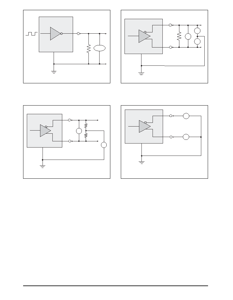
Figure 1. V.28 Driver Output Open Circuit Voltage
Figure 2. V.28 Driver Output Loaded Voltage
Figure 3. V.28 Driver Output Slew Rate
Figure 4. V.28 Driver Output Short-Circuit Current
Figure 6. Driver Output Rise/Fall Times
Figure 5. V.28 Driver Output Power-Off Impedance
TEST CIRCUITS

9
Rev: B Date:7/7/04
SP526 Multi≠Mode Serial Transceiver
© Copyright 2004 Sipex Corporation
Figure 7. V.28 Receiver Input Impedance
A
C
I
ia
±
15V
A
C
V
oc
Figure 8. V.28 Receiver Input Open Circuit Bias
A
V
OC
3.9k
C
A
V
t
450
C
A
C
±
0.25V
V
CC
= 0V
I
x
A
I
sc
C
Figure 9. V.10 Driver Output Open-Circuit Voltage
Figure 10. V.10 Driver Output Test Terminated Voltage
Figure 12. V.10 Driver Output Power-Off Current
Figure 11. V.10 Driver Output Short-Circuit Current
10
Rev: B Date:7/7/04
SP526 Multi≠Mode Serial Transceiver
© Copyright 2004 Sipex Corporation
-
Figure 13. V.10 Driver Output Transition Time
A
450
C
Oscilloscope
Figure 14. V.11 Driver Output Open-Circuit Voltage
A
B
V
OC
3.9k
V
OCA
V
OCB
C
A
B
V
T
50
V
OS
C
50
A
B
C
I
sa
I
sb
Figure 15. V.11 Driver Output Test Terminated Voltage
Figure 16. V.11 Driver Output Short-Circuit Current

11
Rev: B Date:7/7/04
SP526 Multi≠Mode Serial Transceiver
© Copyright 2004 Sipex Corporation
A
B
C
I
xa
±
0.25V
A
B
C
I
xb
±
0.25V
V
CC
= 0V
V
CC
= 0V
A
B
C
I
ia
±
10V
C
I
ib
±
10V
A
B
+3.25mA
≠3.25mA
+10V
+3V
≠3V
≠10V
Maximum Input Current
versus Voltage
V.11 RECEIVER
Figure 17. V.11 Driver Output Power-Off Current
Figure 18. V.11 Receiver Input Current
Figure 19. V.11 Driver Output Rise/Fall Time
Figure 20. V.11 Receiver Input IV Graph
A
B
50
C
50
50
V
E
Oscilloscope

12
Rev: B Date:7/7/04
SP526 Multi≠Mode Serial Transceiver
© Copyright 2004 Sipex Corporation
-
Figure 22. Driver Timing Test Load Circuit
Figure 23. Receiver Timing Test Load Circuit
500
C
L
Output
Under
Test
S
1
S
2
V
CC
1K
1K
C
RL
Receiver
Ou tpu t
S
1
S
2
Test Point
V
CC
Figure 24. Driver Propagation Delays
+3V
0V
DRIVER INPUT
B
A
DRIVER
OUTPUT
V
O
+
DIFFERENTIAL
OUTPUT
V
A
≠ V
B
0V
V
O
≠
1.5V
1.5V
t
PLH
t
R
t
F
f = 1MHz; t
R
10ns; t
F
10ns
V
O
1/2V
O
1/2V
O
t
PHL
t
SKEW
= |t
DPLH
- t
DPHL
|
t
DPHL
t
DPLH
Figure 25. V.11 Driver Enable and Disable Times
+3V
0V
DEC
X
or T
x_
E
nable
5V
V
OL
A, B
0V
1.5V
1.5V
t
ZL
t
ZH
f = 1MHz; t
R
< 10ns; t
F
< 10ns
V
OH
A, B
2.3V
2.3V
t
LZ
t
HZ
0.5V
0.5V
Output normally LOW
Output normally HIGH
Figure 21. Driver/Receiver Timing Test Circuit
C
L1
15pF
RO
A
B
A
B
DI
C
L2
R
L
D
X
or T
X
_Enable

13
Rev: B Date:7/7/04
SP526 Multi≠Mode Serial Transceiver
© Copyright 2004 Sipex Corporation
Figure 27. Receiver Enable and Disable Times
+3V
0V
DEC
X
5V
0V
1.5V
1.5V
t
ZL
t
ZH
f = 1MHz; t
R
10ns; t
F
10ns
RECEIVER OUT
50%
50%
t
LZ
t
HZ
0.5V
0.5V
Output normally LOW
Output normally HIGH
V
IL
V
IH
RECEIVER OUT
D0 or D1
Figure 26. Receiver Propagation Delays
V
OH
V
OL
RECEIVER OUT
50%
t
PLH
f = 1MHz; t
R
10ns; t
F
10ns
OUTPUT
V
OD2
+
V
OD2
≠
A ≠ B
0V
0V
t
PHL
INPUT
50%
t
SKEW
= |t
PHL
- t
PLH
|
Figure 28. V.28 (RS-232) and V.10 Driver Enable and Disable Times
+3V
0V
D
X
or ENT
X
1.5V
1.5V
t
ZL
f = 60kHz; t
R
< 10ns; t
F
< 10ns
T
OUT
t
LZ
Output LOW
0V
+3V
0V
V
OH(MIN)
1.5V
1.5V
t
ZH
f = 60kHz; t
R
< 10ns; t
F
< 10ns
T
OUT
t
HZ
Output HIGH
0V
V
OL(MIN)
D
X
or ENT
X
0.5V
0.5V
0.5V
0.5V

14
Rev: B Date:7/7/04
SP526 Multi≠Mode Serial Transceiver
© Copyright 2004 Sipex Corporation
-
T1
T2
T3
R1
R2
R3
T4
R4
SP526
1.0
µ
F
1.0
µ
F
1.0
µ
F
1.0
µ
F
C2≠
1.0
µ
F
C1+
C1≠
C2+
T1IN
8
ENT1
12
T1OUTA
T1OUTB
T2OUTA
T2OUTB
T2IN
ENT2
ENT3
ENT4
T3IN
T3OUTB
T3OUTA
T4OUT
R1OUT
R2OUT
R3OUT
R4OUT
ENR4
ENR3
ENR1
ENR2
R1INA
R2INA
R3INA
R4INA
R3INB
R4INB
R2INB
R1INB
D0
D1
21
17
19
16
7
11
6
10
5
9
35
4
34
3
33
2
32
1
18
14
13
20
15
22
25
24
27
26
29
28
30
43
42
41
40
39
38
37
36
23
44
31
V
DD
V
CC
V
CC
+5V
V
SS
GND
GND
GND
T4IN
Figure 29. Typical Operating Circuit for the SP526

15
Rev: B Date:7/7/04
SP526 Multi≠Mode Serial Transceiver
© Copyright 2004 Sipex Corporation
THEORY OF OPERATION
The SP526 device is made up of 1) the drivers,
2) the receivers, and 3) a charge pump.
Drivers
The SP526 has four enhanced independent
drivers. Control for the mode selection is done
via a two≠bit control word into DP0 and DP1.
The drivers are prearranged such that for each
mode of operation, the relative position and
functionality of the drivers are set up to
accommodate the selected interface mode. As
the mode of the drivers is changed, the electrical
characteristics will change to support the
required signal levels. The mode of each driver
in the different interface modes that can be
selected is shown in Table 1.
There are four basic types of driver circuits --
RS-232 (V.28), RS-423 (V.10), RS-422 (V.11),
and RS-485.
The RS-232 (V.28) drivers output single≠ended
signals with a minimum of
±5V (with 3K &
2500pF loading), and can operate to at least
120Kbps. Since the SP526 uses a charge pump
to generate the RS-232 output rails, the driver
outputs will never exceed
±10V.
The RS-423 (V.10) drivers are also single≠
ended signals which produce open circuit V
OL
and V
OH
measurements of
±4.0V to ±6.0V.
When terminated with a 450
load to ground,
the driver output will not deviate more than 10%
of the open circuit value. This is in compliance
FEATURES
The SP526 contains highly integrated serial
transceivers that offer programmability between
interface modes through software control. The
SP526 offers the hardware interface modes for
RS-232 (V.28), RS-423 (V.10), RS-422 (V.11),
and RS-485. The interface mode selection is
done via two control pins.
The SP526 has four drivers, four receivers, and
an on-board charge pump that is ideally suited
for low-cost wide area network connectivity
and other multi-protocol applications. Based on
our multi-mode SP500 family, Sipex has
allocated specific transceiver cells, or "building
blocks," from this product series and created the
SP526. Sipex's "building blocks" concept
allows these small transceiver cells to be
packaged to offer a simple low-cost solution to
networking applications that need only 4
interface modes. For example, an 8-channel
applications requiring eight serial transceivers
can be achieved implementing two SP526
devices. The SP526 can be implemented in
series with other devices in our SP500 family.
A 9-channel network application can be achieved
implementing the SP505 which contains seven
transceivers in conjunction with the SP526.
1
D
0
D
S
R
E
V
I
R
D
S
R
E
V
I
E
C
E
R
1
T
2
T
3
T
4
T
1
R
2
R
3
R
4
R
0
0
e
d
o
M
e
t
a
t
S
-
i
r
T
n
i
s
t
u
p
t
u
O
x
R
d
n
a
x
T
-
N
W
O
D
T
U
H
S
0
1
1
1
.
V
1
1
.
V
1
1
.
V
0
1
.
V
1
1
.
V
1
1
.
V
1
1
.
V
1
1
.
V
1
0
1
1
.
V
1
1
.
V
0
1
.
V
0
1
.
V
1
1
.
V
1
1
.
V
1
1
.
V
1
1
.
V
1
1
8
2
.
V
8
2
.
V
8
2
.
V
8
2
.
V
8
2
.
V
8
2
.
V
8
2
.
V
8
2
.
V
Table 1. SP526 Driver and Receiver Mode Selection with the Control Lines D1 and D0

16
Rev: B Date:7/7/04
SP526 Multi≠Mode Serial Transceiver
© Copyright 2004 Sipex Corporation
-
of the ITU V.10 specification. The RS-423
drivers are used in RS-449, EIA-530, EIA-530A
and V.36 modes as Category II signals from
each of their corresponding specifications.
The third and fourth type of drivers are RS-422
(V.11)/RS-485 type differential drivers. Due to
the nature of differential signaling, the drivers
are more immune to noise as opposed to single-
ended transmission methods. The advantage is
evident over high speeds and long transmission
lines. The strength of the driver outputs can
produce differential signals that can maintain
RS-485,
±1.5V differential output levels with a
worst case load of 54
. The signal levels and
drive capability of these drivers allow the driv-
ers to also support RS-422 (V.11) requirements
of
±2V differential output levels with 100
loads. The driver is designed to operate over a
common mode range of +7V to -7V which
follows the V.11 specification. The RS-422
drivers are used in RS-449, EIA-530, EIA-530A
and V.36 modes as Category I signals which are
used for clock and data. All of the differential
drivers can operate to at least 10Mbps.
The drivers also have separate enable pins which
simplifies half-duplex configurations for some
applications and also provides simpler DTE/
DCE flexibility with one integrated circuit. The
enable pins will tri-state the drivers when the
ENT1, ENT2, ENT3, and ENT4 pins are at a
logic HIGH ("1"). During tri-stated conditions,
the driver outputs will be at a high impedance
state.
The driver inputs are both TTL or CMOS com-
patible. Each driver input should have a pull-
down or pull-up resistor so that the output will
be at a defined state. Unused driver inputs
should have pull-up resistors to +5V connected
so that the output is at a logic LOW ("0").
Unused driver inputs should not be left floating.
For differential drivers, the non-inverting out-
put will be at a logic HIGH ("1"). The typical
pull-up resistor value should be 400k
.
Receivers
The SP526 has four independent receivers which
can be programmed for the different interface
modes. Control for the mode selection is done
via a two≠bit control word that is the same as the
driver control word. Therefore, if the modes for
the drivers and receivers are supposed to be
identical in the application, the control lines can
be tied together.
Like the drivers, the receivers are prearranged
for the specific requirements of the synchronous
serial interface. As the operating mode of the
receivers is changed, the electrical characteris-
tics will change to support the required serial
interface protocols of the receivers. Table 1
shows the mode of each receiver in the different
interface modes that can be selected.
There are two basic types of receiver circuits --
RS-232 (V.28) and RS-422 (V.11).
The RS-232 (V.28) receiver is single≠ended and
accepts RS-232 signals from the RS-232 driver.
The RS-232 receiver has an operating voltage
range of
±15V and can receive signals downs to
±3V. The input sensitivity complies with RS-
232 and V.28 at
±3V. The input impedance is
3k
to 7k in accordance to RS-232 and V.28.
The receiver output produces a TTL/CMOS
signal with a +2.4V minimum for a logic "1" and
a +0.8V maximum for a logic "0". RS-232(V.28)
receivers can be used in RS-232 mode for data,
clock or control signals. They are also used in
V.35 mode for control line signals: CTS, DSR,
LL, and RL. The RS-232 receivers can operate
to at least 120kbps.

17
Rev: B Date:7/7/04
SP526 Multi≠Mode Serial Transceiver
© Copyright 2004 Sipex Corporation
The third type of receiver is a differential which
supports RS-422/V.11 signals. This receiver
has a typical input impedance of 10K
and a
differential threshold of
±0.3V, which complies
with the RS-422/V.11 specifications. Since the
characteristics of the RS-422 (V.11) receivers
are actually subsets of RS-485, the RS-422/
V.11 receivers can accept RS-485 signals.
However, these receivers cannot support 32
transceivers on the signal bus due to the lower
input impedance as specified in the RS-485
specifications. V.11 receivers are used in
RS-422, RS-449, EIA-530, EIA-530A and V.36
as Category I signals for receiving clock, data,
and some control line signals not covered
by Category II V.10 circuits. The differential
receivers can receive signals up to at least
10Mbps.
All four receivers include an enable line for
tri-state of the receiver output allowing
convenient half-duplex configurations. When
the enable lines are at a logic LOW ("0") active,
the receiver outputs are high impedance and will
be at approximately 10k
during tri-state.
All receivers include a fail-safe feature that
outputs a logic high when the receiver inputs are
open. For single-ended RS-232 receivers, there
are internal 5k
pull-down resistors on the
inputs which produces a logic high ("1") at the
receiver outputs. The single-ended RS-423
receivers produce a logic LOW ("0") on the
output when the inputs are open. This is due to
a pull-up device connected to the input. The
differential receivers have the same internal
pull-up device on the non-inverting input which
produces a logic HIGH ("1") at the receiver output.
Charge Pump
The charge pump is a Sipex≠patented design
(U.S. 5,306,954) and uses a unique approach
compared to older less≠efficient designs. The
charge pump still requires four external capaci-
tors, but uses a four≠phase voltage shifting
technique to attain symmetrical 10V power
supplies. There is a free≠running oscillator that
controls the four phases of the voltage shifting.
A description of each phase follows.
Phase 1
-- V
SS
charge storage --During this phase of
the clock cycle, the positive side of capacitors
C
1
and C
2
are initially charged to +5V. C
l
+
is
then switched to ground and the charge in C
1
≠
is
transferred to C
2
≠
. Since C
2
+
is connected to
+5V, the voltage potential across capacitor C
2
is
now 10V.
Phase 2
-- V
SS
transfer -- Phase two of the clock
connects the negative terminal of C
2
to the V
SS
storage capacitor and the positive terminal of C
2
to ground, and transfers the generated ≠l0V to
C
3
. Simultaneously, the positive side of
capacitor C
1
is switched to +5V and the
negative side is connected to ground.
Phase 3
-- V
DD
charge storage -- The third phase of the
clock is identical to the first phase -- the charge
transferred in C
1
produces ≠5V in the negative
terminal of C
1
, which is applied to the negative
side of capacitor C
2
. Since C
2
+
is at +5V, the
voltage potential across C
2
is l0V.
C
1
+
-
-5V
V
CC
= +5V
+5V
C
2
-5V
C
4
C
3
+
-
+
-
-
+
V
DD
Storage Capacitor
V
SS
Storage Capacitor
Figure 30. Charge Pump -- Phase 1

18
Rev: B Date:7/7/04
SP526 Multi≠Mode Serial Transceiver
© Copyright 2004 Sipex Corporation
-
Figure 31. Charge Pump -- Phase 2
C
1
+
-
V
CC
= +5V
C
2
-10V
C
4
C
3
+
-
+
-
-
+
V
DD
Storage Capacitor
V
SS
Storage Capacitor
Figure 32. Charge Pump Waveforms
+10V
a) C
2
+
GND
GND
b) C
2
≠
≠10V
Figure 33. Charge Pump -- Phase 3
C
1
+
-
-5V
V
CC
= +5V
+5V
C
2
-5V
C
4
C
3
+
-
+
-
-
+
V
DD
Storage Capacitor
V
SS
Storage Capacitor
Figure 34. Charge Pump -- Phase 4
C
1
+
-
V
CC
= +5V
+10V
C
2
C
4
C
3
+
-
+
-
-
+
V
DD
Storage Capacitor
V
SS
Storage Capacitor

19
Rev: B Date:7/7/04
SP526 Multi≠Mode Serial Transceiver
© Copyright 2004 Sipex Corporation
Phase 4
-- V
DD
transfer -- The fourth phase of the clock
connects the negative terminal of C
2
to ground,
and transfers the generated l0V across C
2
to C
4
,
the V
DD
storage capacitor. Again, simultaneously
with this, the positive side of capacitor C
1
is
switched to +5V and the negative side is con-
nected to ground, and the cycle begins again.
Since both V
+
and V
≠
are separately generated
from V
CC
; in a no≠load condition V
+
and V
≠
will
be symmetrical. Older charge pump approaches
that generate V
≠
from V
+
will show a decrease in
the magnitude of V
≠
compared to V
+
due to the
inherent inefficiencies in the design.
The clock rate for the charge pump typically
operates at 15kHz. The external capacitors can
be as low as 1.0
µF with a 16V breakdown
voltage rating.
ESD Tolerance
The SP526 device incorporates ruggedized
ESD cells on all driver output and receiver input
pins. The ESD structure is improved over our
previous family for more rugged applications
and environments sensitive to electro-static
discharges and associated transients. The
improved ESD tolerance is at least
±15kV
without damage nor latch-up.
There are different methods of ESD testing
applied:
a) MIL-STD-883, Method 3015.7
b) IEC1000-4-2 Air-Discharge
c) IEC1000-4-2 Direct Contact
The Human Body Model has been the generally
accepted ESD testing method for semiconductors.
This method is also specified in MIL-STD-883,
Method 3015.7 for ESD testing. The premise of
this ESD test is to simulate the human body's
potential to store electro-static energy and
discharge it to an integrated circuit. The
simulation is performed by using a test model as
shown in Figure 35. This method will test the
IC's capability to withstand an ESD transient
during normal handling such as in manufacturing
areas where the ICs tend to be handled frequently.
The IEC-1000-4-2, formerly IEC801-2, is
generally used for testing ESD on equipment and
systems. For system manufacturers, they must
guarantee a certain amount of ESD protection
since the system itself is exposed to the outside
environment and human presence. The premise
with IEC1000-4-2 is that the system is required
to withstand an amount of static electricity when
ESD is applied to points and surfaces of the
equipment that are accessible to personnel during
normal usage. The transceiver IC receives most
R
C
SW
DC Power
Source
C
S
R
S
SW2
Device
Under
Test
Figure 35. ESD Test Circuit for Human Body Model

20
Rev: B Date:7/7/04
SP526 Multi≠Mode Serial Transceiver
© Copyright 2004 Sipex Corporation
-
30A
15A
0A
t=0nS
t=30nS
t
Figure 37. ESD Test Waveform for IEC1000-4-2
of the ESD current when the ESD source is
applied to the connector pins. The test circuit for
IEC1000-4-2 is shown on Figure 36. There are
two methods within IEC1000-4-2, the Air
Discharge method and the Contact Discharge
method.
With the Air Discharge Method, an ESD voltage
is applied to the equipment under test (EUT)
through air. This simulates an electrically charged
person ready to connect a cable onto the rear of
the system only to find an unpleasant zap just
before the person touches the back panel. The
high energy potential on the person discharges
through an arcing path to the rear panel of the
system before he or she even touches the system.
This energy, whether discharged directly or
through air, is predominantly a function of the
discharge current rather than the discharge
voltage. Variables with an air discharge such as
approach speed of the object carrying the ESD
Table 2. Transceiver ESD Tolerance Levels
Device Pin
Human Body
IEC1000-4-2
Tested
Model
Air Discharge Direct Contact Level
Driver Outputs
±
15kV
±
15kV
±
8kV
4
Receiver Inputs
±
15kV
±
15kV
±
8kV
4
R
C
C
S
R
S
R
V
SW1
SW2
Contact-Discharge Module
Device
Under
Test
DC Power
Source
RS and RV add up to 330
for IEC1000-4-2
Figure 36
.
ESD Test Circuit for IEC1000-4-2

21
Rev: B Date:7/7/04
SP526 Multi≠Mode Serial Transceiver
© Copyright 2004 Sipex Corporation
potential to the system and humidity will tend to
change the discharge current. For example, the
rise time of the discharge current varies with the
approach speed.
The Contact Discharge Method applies the ESD
current directly to the EUT. This method was
devised to reduce the unpredictability of the
ESD arc. The discharge current rise time is
constant since the energy is directly transferred
without the air-gap arc. In situations such as
hand held systems, the ESD charge can be directly
discharged to the equipment from a person already
holding the equipment. The current is transferred
on to the keypad or the serial port of the equipment
directly and then travels through the PCB and
finally to the IC.
The circuit models in Figures 35 and 36 represent
the typical ESD testing circuits used for all three
methods. The C
S
is initially charged with the DC
power supply when the first switch (SW1) is on.
Now that the capacitor is charged, the second
switch (SW2) is on while SW1 switches off. The
voltage stored in the capacitor is then applied
through R
S
, the current limiting resistor, onto the
device under test (DUT). In ESD tests, the SW2
switch is pulsed so that the device under test
receives a duration of voltage.
For the Human Body Model, the current limiting
resistor (R
S
) and the source capacitor (C
S
) are
1.5k
an 100pF, respectively. For IEC-1000-4-
2, the current limiting resistor (R
S
) and the source
capacitor (C
S
) are 330
an 150pF, respectively.
The higher C
S
value and lower R
S
value in the
IEC1000-4-2 model are more stringent than the
Human Body Model. The larger storage capacitor
injects a higher voltage to the test point when
SW2 is switched on. The lower current limiting
resistor increases the current charge onto the test
point.
NET1/NET2 European Compliancy
As with all of Sipex's previous multi-protocol
serial transceiver ICs, the drivers and receivers
have been designed to meet all the requirements
to NET1/NET2. The SP526 is also tested and
adheres to all the NET1/2 physical layer testing
and the ITU Series V specifications. Please note
that although the SP526, as with its predecessors,
adheres to NET1/2 testing, any complex or
unusual configuration should be double-checked
to ensure NET compliance. Consult the factory
for details.
22
Rev: B Date:7/7/04
SP526 Multi≠Mode Serial Transceiver
© Copyright 2004 Sipex Corporation
-
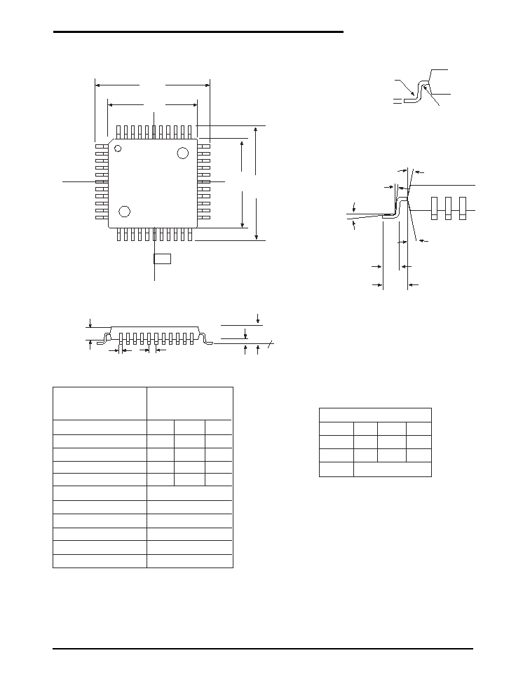
PACKAGE:44 PIN LQFP
44 PIN LQFP
L
11
∞
- 13
∞
0
∞
Min
11
∞
- 13
∞
0
∞
≠7
∞
DIMENSIONS
Minimum/Maximum
(mm)
SYMBOL
A
A1
A2
b
D
D1
e
E
E1
N
44≠PIN LQFP
JEDEC MS-026
(BCB) Variation
MIN
NOM
MAX
1.60
0.05
0.15
1.35
1.40
1.45
0.30
0.37
0.50
12.00 BSC
10.00 BSC
0.80 BSC
12.00 BSC
10.00 BSC
44
c
L1
COMMON DIMENTIONS
SYMBL MIN
NOM
MAX
c
0.11
23.00
L
0.73
0.88
1.03
L1
0.25 BASIC
b
e
A2
0.2 RAD. MAX.
0.08 RAD. MIN.
Seating
Plane
A1
A
A
E
1
D
1
D
CL
CL
-D-
Pin 1
E

23
Rev: B Date:7/7/04
SP526 Multi≠Mode Serial Transceiver
© Copyright 2004 Sipex Corporation
ORDERING INFORMATION
Part Number
Temperature Range
Package Types
SP526CF ........................................................................... 0
∞
C to +70
∞
C ............................................................................... 44≠pin JEDEC LQFP
Corporation
ANALOG EXCELLENCE
Sipex Corporation reserves the right to make changes to any products described herein. Sipex does not assume any liability arising out of the
application or use of any product or circuit described herein; neither does it convey any license under its patent rights nor the rights of others.
Please consult the factory for pricing and availability on a Tape-On-Reel option.
Sipex Corporation
Headquarters and
Sales Office
233 South Hillview Drive
Milpitas, CA 95035
TEL: (408) 934-7500
FAX: (408) 935-7600
Sales Office
22 Linnell Circle
Billerica, MA 01821
TEL: (978) 667-8700
FAX: (978) 670-9001
e-mail: sales@sipex.com
DATE
REVISION
DESCRIPTION
1/27/04
A
Implemented tracking revision.
7/7/04
B
Available in LQFP package.
REVISION HISTORY
Available in lead free packaging. To order add "-L" suffix to part number.
Example: SP526CF = standard; SP526CF-L = lead free